TYBT1 Reset & Teardown (FCC ID 2ANDL-TYBT1)
Factory reset and internal photos for Tuya Global TYBT1. Tuya / Smart Life smart plug.
January 15, 2026
•
8 read

Before you buy the Tuya Global TYBT1, check what's inside.
The Tuya TYBT1 is a compact Bluetooth Low Energy (BLE) module designed for controlling LED lighting. It features a TLSR8266 chipset and offers PWM, I2C, and UART interfaces for custom LED product integration.
⚠️ NOTE: Ensure correct battery polarity when installing and operating.
Quick Specs
- Manufacturer: Tuya Global
- Model: TYBT1
- Protocol: Bluetooth
- Chipset: Tuya BLE
- Ecosystem: Tuya / Smart Life
- App: Smart Life
🔧 Geek Corner (Flashing Info)
- Chipset: TLSR8266
- Flashable: ❌ No
- Info: The firmware is BLE only and likely proprietary, not designed for flashing with custom firmware like Tasmota.
User Manual
Scanned pages from the official user manual:

External Photos
Photos of the device exterior:

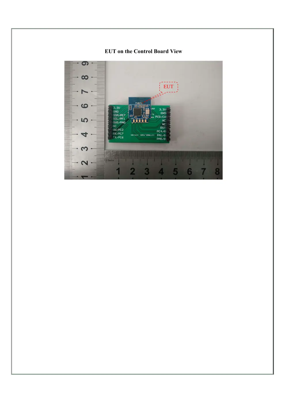
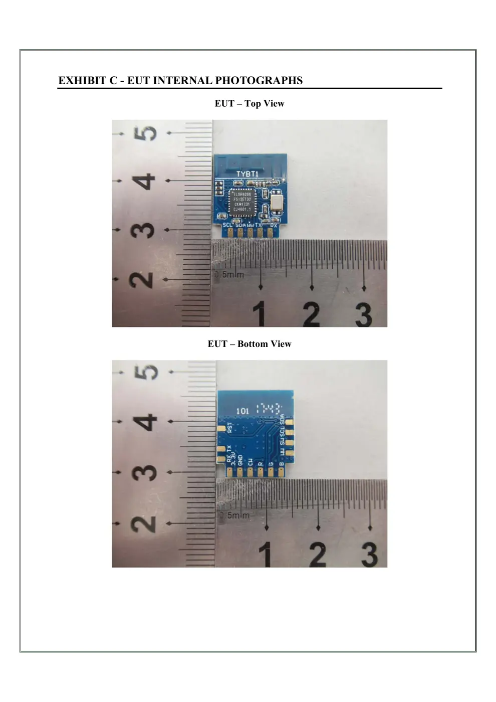
Internal Photos
Teardown photos showing the PCB and components:
Verdict
The TYBT1 is a Bluetooth device from the Tuya / Smart Life ecosystem.
📄 Click to view full text manual (SEO)
Intellige
nt
TYBT1 DATASHEET
TYBT1 User Manual
1. Product Overview
TYBT1 is a Bluetooth (BLE) module desi gned by Hangzhou AiXiangJi Technology Co., Ltd,
which is designed for outputting LED control signals. The BLE Module consists of a highly
integrated wireless Bluetooth chip TLSR8266 and some extra electric circuits that have been
programed with Bluetooth network protocol and plenty of software examples. TYBT1 include a
32-bit CPU, BLE, 512K byte flash, 1 6k SRAM , 5 -channel PWM , one I2C and one
UART interface.
Users can customize their LED products by using these PWM signals .
1.1 Features
² Integrated low power consumption 32 -bit CPU, also known as application processor
² Basic frequency of the CPU can support 48 MHz
² Supply voltage range: 1.9V to 3.6V
² Peripherals: 5*PWM,1*I2C, 1*UART
² BLE RF features:
l Compatible with BLE 4.0
l
TX transmitting power: 6.0 dBm
l RX receiving sensitivity: -92dBm
l AES hardware encryption
l On-board PCB an tenna
l Operating temperature range: -20℃ to 85℃
1.2 Main Application Fields
² LED
² Intelligent household applications
TYBT1 DAT
ASHEET
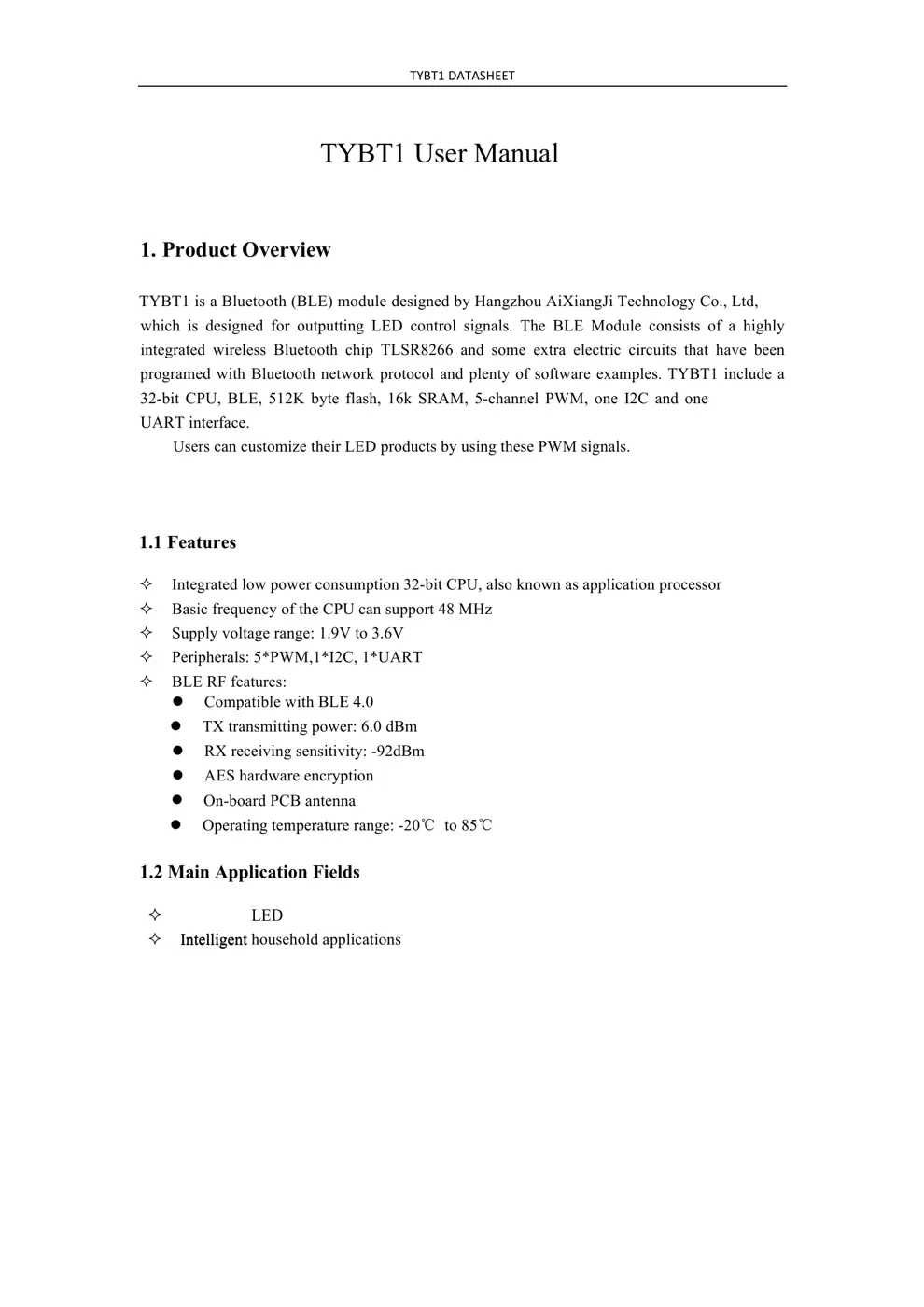
2. Dim
ensions and Footprint
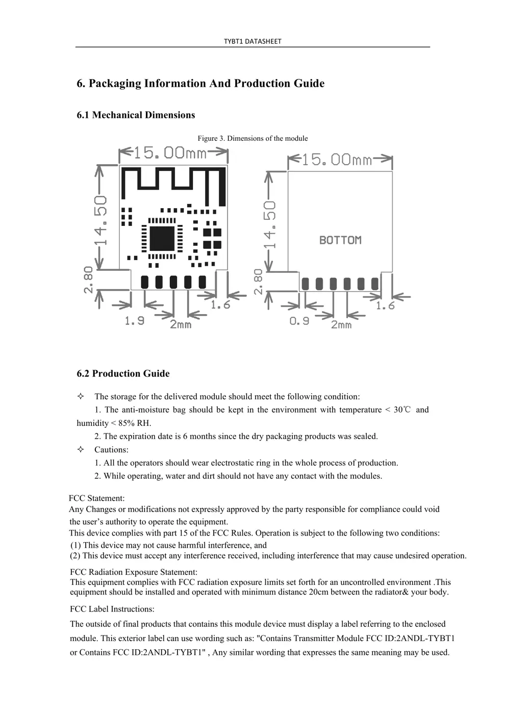
2.1 Dimensions
TYB
T1 have double sides of golden finger pins . The distance between each Pin is 2.0mm.
Size of TYBT1: 15mm(W)*17.3mm(L).
Figure 2 shows the dimensions of TYBT1.
Fig
ure 2. The dimensions of TYBT1
2.2 Pin Definition
Tab
le 1 shows the general pin attributes of TYBT1
Tab
le 1. The typical pin definition of TYBT1
PIN
NO. NAME TYPE DESCRIPTION
1 3.
3V P Supply voltage
2,14
RX I UART RX
3 GND
P Ground
4,13
TX O UART TX
5 CW I/
O PWM output pin, default for Cold White LED line
6,15
WW I/O PWM output pin, default for Warm White LED line
7
R I/O PWM output pin, default for Red LED line
8,18
SDA I/O I2C, data interface
9
G I/O PWM output pin, default for Green LED line
10,17
SCL I/O I2C, clock interface
11 B I/
O PWM output pin, default for Blue LED line
12 RST
I Reset pin for the module
16 SW I/O Bl
uetooth chipset burning pin
Note:
S: Power supply pins; I/O: Digital input or output pins .
If there’s any customization needed for PWM output, please contact our BD manager.
TYBT1 DATA
SHEET
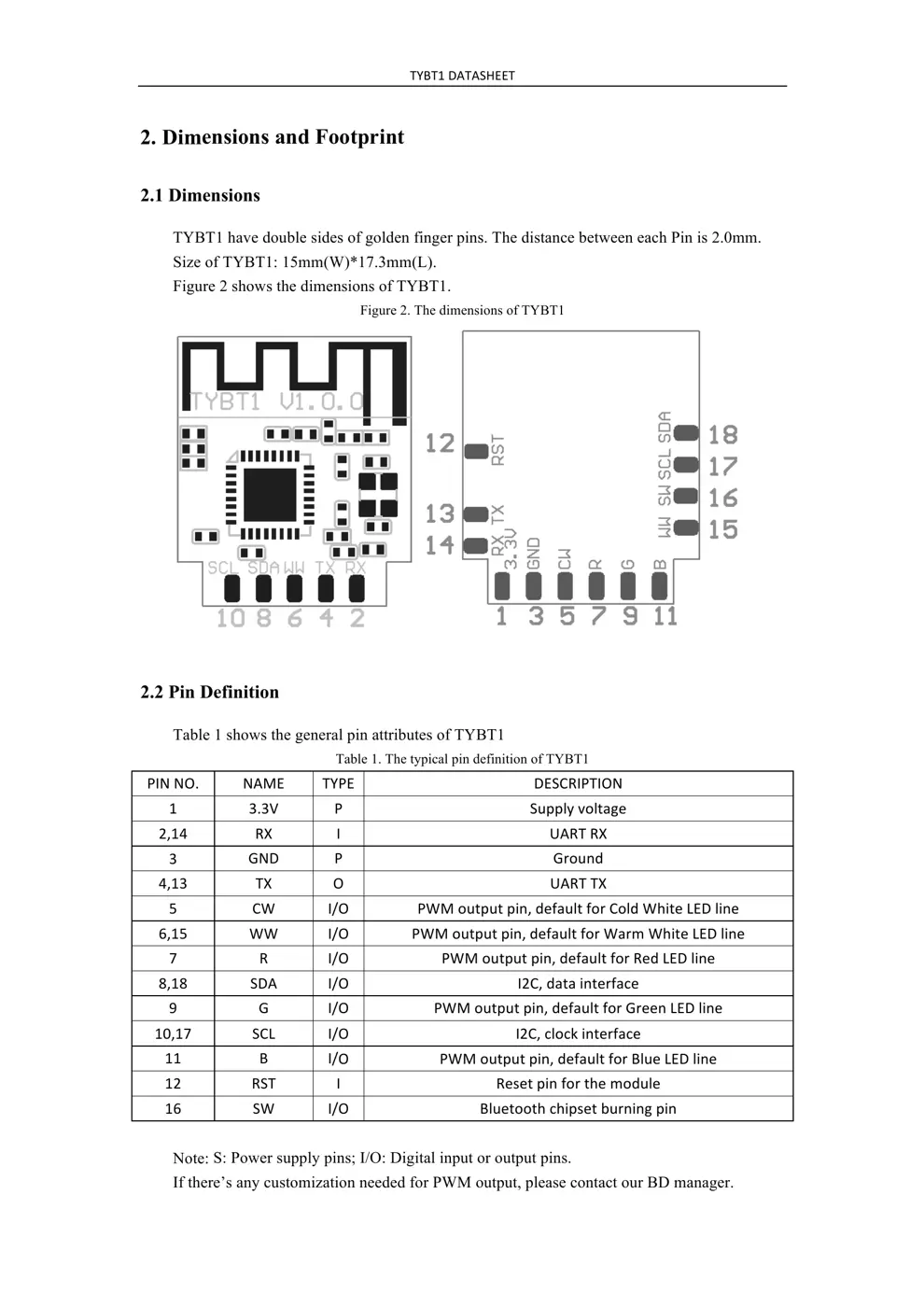
3. Elec
trical Characteristics
3.1 Absolute Maximum Ratings
Table
2. Absolute Maximum Ratings
PARAM
ETERS DESCRIPTION MIN MAX UNI
T
Ts Stor
age
temperature
-20 85 ℃
VCC Supply voltage 1.9 3.6 V
Elec
trostatic release quantity
(Human body model)
TAMB-25℃ - 2 KV
Elec
trostatic release quantity
(Machine model)
TAMB-25℃ - 0.5 KV
3.2 Electrical Conditions
Table
3. Electrical Conditions
PARAM
ETERS DESCRIPTION MIN TYPIC
AL
MAX UNIT
Ta Temp
erature for Commercial grade - 20 - 85 ℃
VCC Sup
ply voltage 1.9 3.3 3.6 V
VIL IO n
egative level input - 0.3 - VCC*0.25 V
VIH IO p
ositive level input VCC*0.75 - VCC V
VOL IO n
egative level output - - VCC*0.1 V
VoH IO p
ositive level output VCC*0.8 - VCC V
3.3 Transmitting Current Consumptions
Tabl
e 4. TX current consumption
PARAM
ETERS MO...