TYZS1L Reset & Teardown (FCC ID 2ANDL-TYZS1L)
Factory reset and internal photos for Tuya Global TYZS1L. Tuya / Smart Life smart plug.
January 15, 2026
•
8 read
Before you buy the Tuya Global TYZS1L, check what's inside.
The Tuya TYZS1L is a low-power embedded Zigbee module featuring an EFR32MG13P732HI ARM Cortex-M4 processor. It is designed for integration into smart home devices, offering Zigbee connectivity and operating on low battery voltage.
⚠️ NOTE: Ensure correct battery polarity and voltage (1.8V-3.8V).
Quick Specs
- Manufacturer: Tuya Global
- Model: TYZS1L
- Protocol: Zigbee
- Chipset: Tuya Zigbee
- Ecosystem: Tuya / Smart Life
- App: Smart Life
🔧 Geek Corner (Flashing Info)
- Chipset: EFR32MG13P732HI
- Flashable: ❌ No
- Info: Proprietary Tuya Zigbee module, not designed for user firmware flashing.
User Manual
Scanned pages from the official user manual:
External Photos
Photos of the device exterior:
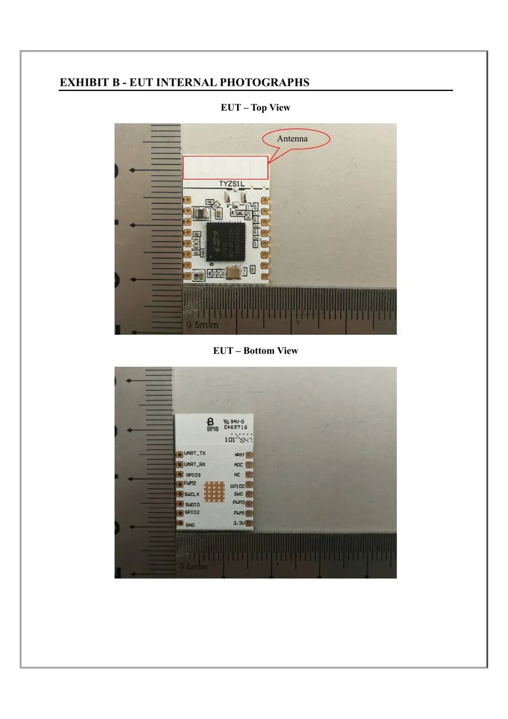
Internal Photos
Teardown photos showing the PCB and components:
Verdict
The TYZS1L is a Zigbee device from the Tuya / Smart Life ecosystem.
📄 Click to view full text manual (SEO)
TYZS1L User manual
Version1.0.0 1
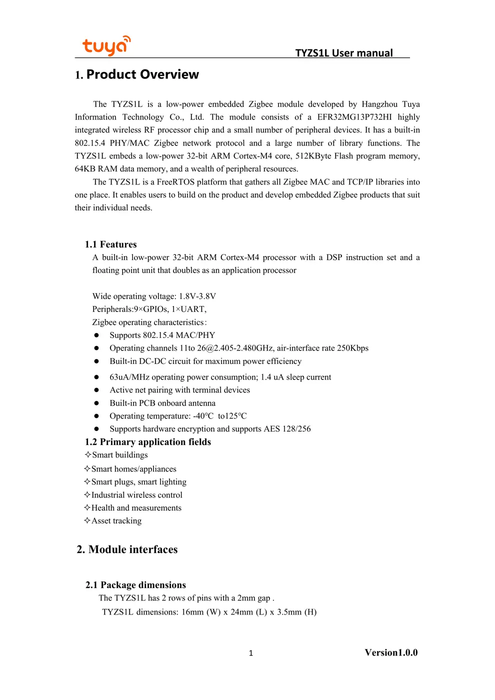
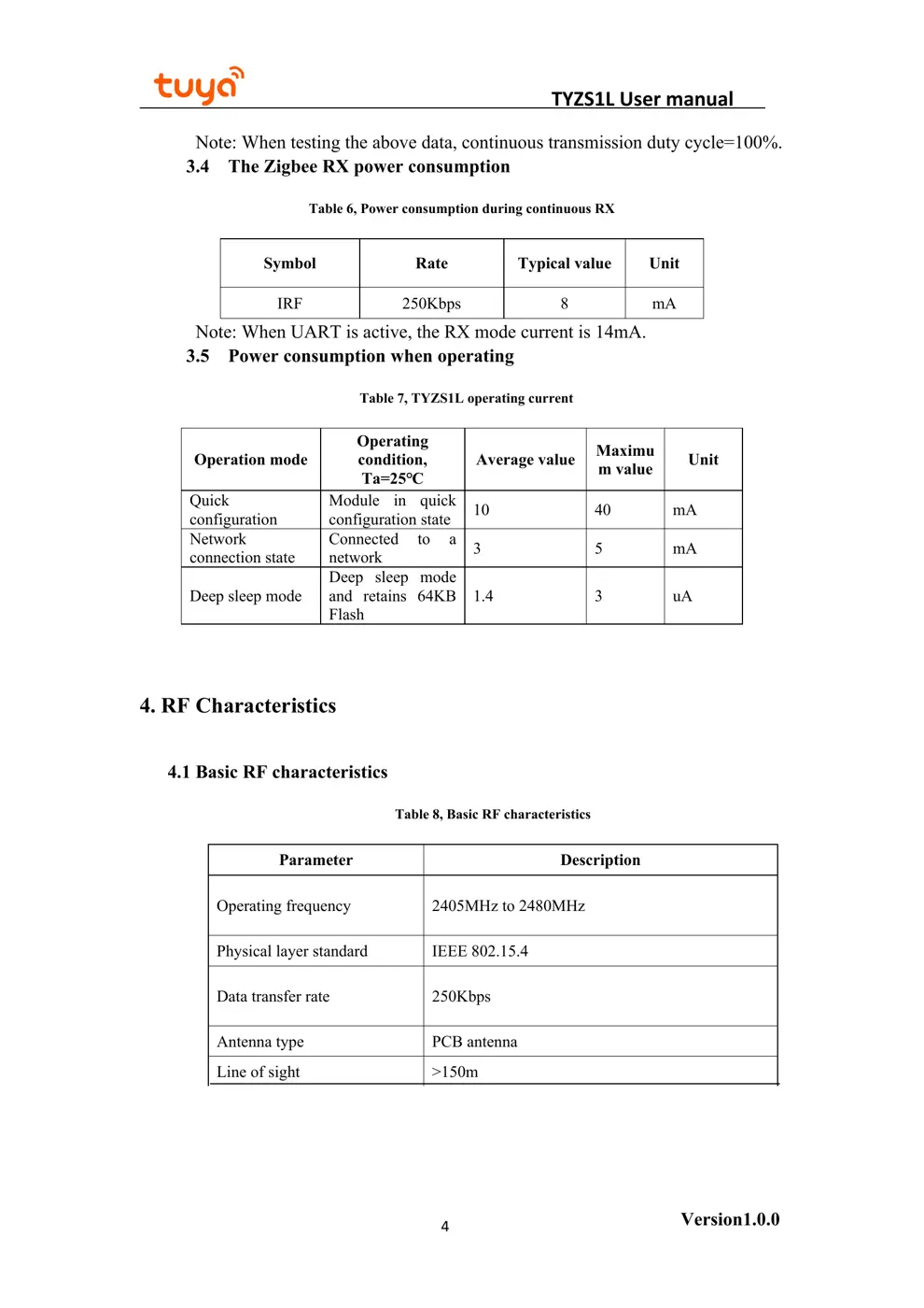
1. Product Overview
The TYZS1L is a low-power embedded Zigbee module developed by Hangzhou Tuya
Information Technology Co., Ltd. The module consists of a EFR32MG13P732HI highly
integrated wireless RF processor chip and a small number of peripheral devices. It has a built-in
802.15.4 PHY/MAC Zigbee network protocol and a large number of library functions. The
TYZS1L embeds a low-power 32-bit ARM Cortex-M4 core, 512KByte Flash program memory,
64KB RAM data memory, and a wealth of peripheral resources.
The TYZS1L is a FreeRTOS platform that gathers all Zigbee MAC and TCP/IP libraries into
one place. It enables users to build on the product and develop embedded Zigbee products that suit
their individual needs.
1.1 Features
A built-in low-power 32-bit ARM Cortex-M4 processor with a DSP instruction set and a
floating point unit that doubles as an application processor
Wide operating voltage: 1.8V-3.8V
Peripherals:9×GPIOs, 1×UART,
Zigbee operating characteristics:
Supports 802.15.4 MAC/PHY
Operating channels 11to [email protected], air-interface rate 250Kbps
Built-in DC-DC circuit for maximum power efficiency
63uA/MHz operating power consumption; 1.4 uA sleep current
Active net pairing with terminal devices
Built-in PCB onboard antenna
Operating temperature: -40℃ to 125℃
Supports hardware encryption and supports AES 128/256
1.2 Primary application fields
Smart buildings
Smart homes/appliances
Smart plugs, smart lighting
Industrial wireless control
Health and measurements
Asset tracking
2. Module interfaces
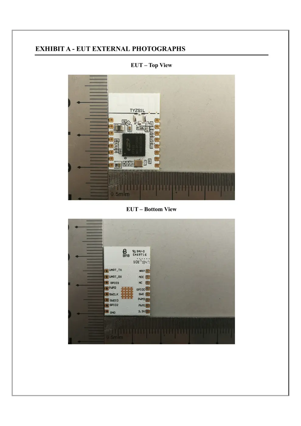
2.1 Package dimensions
The TYZS1L has 2 rows of pins with a 2mm gap .
TYZS1L dimensions: 16mm (W) x 24mm (L) x 3.5mm (H).
TYZS1L User manual
Version1.0.02
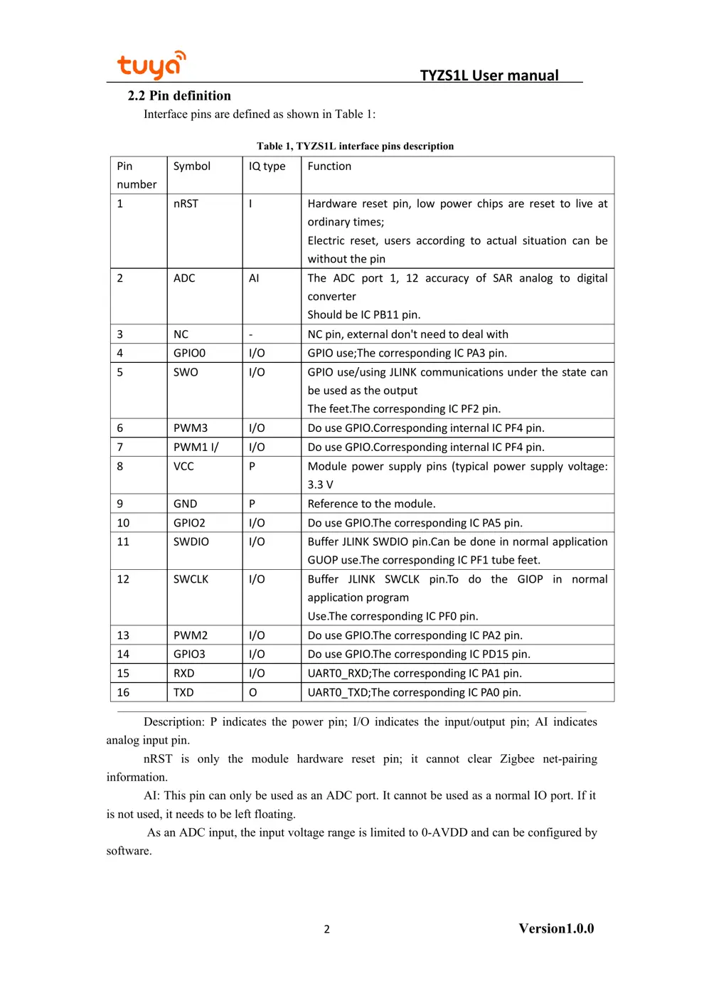
2.2 Pin definition
Interface pins are defined as shown in Table 1:
Table 1, TYZS1L interface pins description
Description: P indicates the power pin; I/O indicates the input/output pin; AI indicates
analog input
pin.
nRST is only the module hardware reset pin; it cannot clear Zigbee net-pairing
information.
AI: This pin can only be used as an ADC port. It cannot be used as a normal IO port. If it
is not used, it needs to be left floating.
As an ADC input, the input voltage range is limited to 0-AVDD and can be configured by
software.
Pin
number
Symbol IQ type Function
1 nRST I Hardware reset pin, low power chips are reset to live at
ordinary times;
Electric reset, users according to actual situation can be
without the pin
2 ADC AI The ADC port 1, 12 accuracy of SAR analog to digital
converter
Should be IC PB11 pin.
3 NC - NC pin, external don't need to deal with
4 GPIO0 I/O GPIO use;The corresponding IC PA3 pin.
5 SWO I/O GPIO use/using JLINK communications under the state can
be used as the output
The feet.The corresponding IC PF2 pin.
6 PWM3 I/O Do use GPIO.Corresponding internal IC PF4 pin.
7 PWM1 I/ I/O Do use GPIO.Corresponding internal IC PF4 pin.
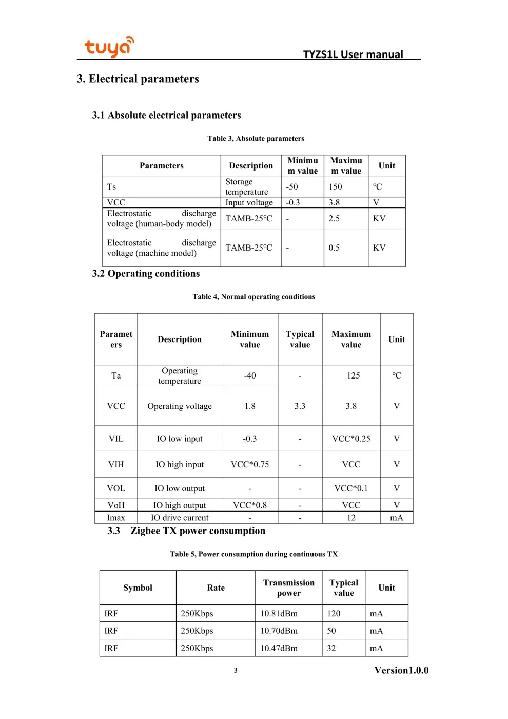
8 VCC P Module power supply pins (typical power sup...